Technology
With substantially larger chip sizes for emerging 3D sensing and consumer applications, the ability to add capacity and scale for volume production is critical. Vertilite’s proprietary wafer technology enables and accommodates customer-focused foundry services. Our dedicated 6” wafer foundries have cutting-edge technology and high-end facilities to fabricate standard and custom devices.

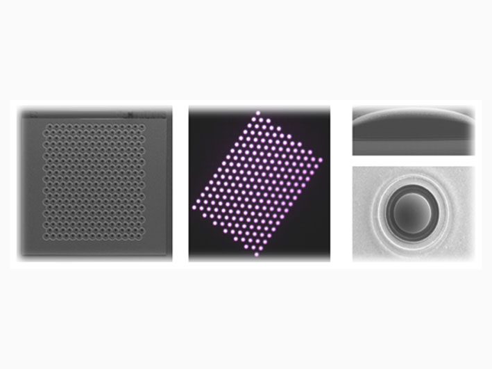
Figure 1. SEM images of VCSEL array (left), near field (middle), and VCSEL with wafer-level microlens for beam shaping (right).
